Table of Contents
The Bottom Line for Procurement Teams
Below 3 nanometers, trace ionic contamination in ultrapure water costs millions per incident in yield. A modern fab consumes up to 15 million gallons of water a day, and roughly 75 percent of that is processed into UPW that has to hold 18.2 MΩ·cm resistivity at the point of use. Every dissolved ion, every particle, and every organic molecule that reaches a wafer surface during a wet clean is a potential yield killer.
Shanghai ChiMay’s in-line conductivity monitoring is built for that environment, delivering continuous sub-ppb-level sensitivity while cutting five-year total cost of ownership by 25 to 35 percent compared with fragmented multi-vendor deployments. That is the basis on which the procurement decision should be made — five-year cost, not unit price — because calibration, maintenance, spare parts, and unplanned downtime compound quickly across the dozens of monitoring points an advanced fab runs.
The market backdrop is simple: WSTS projects the global semiconductor market will exceed $1.51 trillion in 2026, roughly 90 percent growth year over year, driven by AI infrastructure. Global chip sales alone reached $146.8 billion in July 2026, the seventeenth consecutive month of sequential growth. Every new fab needs water quality monitoring from day one, and every fab upgrading to an advanced node needs monitoring that can hold tighter purity specifications.
Why Point-of-Use Conductivity Monitoring Is Non-Negotiable
The Physics of Contamination at Advanced Nodes
At 3nm and below, ionic contaminants at parts-per-trillion concentrations can nucleate defects on wafer surfaces during wet cleaning. TSMC has described the purity required at advanced nodes in terms an operator can picture: roughly no more than 1 milliliter of impurity in 1,000 Olympic-sized swimming pools of water. Grab sampling introduces delay — by the time lab results come back, contaminated water may already have processed wafers worth millions. Continuous in-line conductivity monitoring closes that gap by catching resistivity deviation as it happens.
Advanced fabs running processes below 7nm account for a large and growing share of US ultrapure water demand, and their purification requirements are substantially higher than those of legacy nodes. The monitoring infrastructure has to match that intensity, which means detecting not just whether water is in specification, but the earliest trend that says it is about to leave specification.
What Specification Compliance Requires
Semiconductor-grade UPW is defined by resistivity of 18.2 MΩ·cm — about 0.055 μS/cm at 25°C, the practical limit for water. The relevant Chinese standard, GB/T 11446.1-2013, sets EW-I grade at resistivity of at least 18 MΩ·cm (with the theoretical ceiling at 18.2 MΩ·cm), TOC of no more than 20 μg/L, and sodium of no more than 0.5 μg/L. Holding those numbers consistently requires monitoring with a 0.01 cm⁻¹ cell constant and resolution down to 0.001 μS/cm. Large fabs in the 500-1,000 m³/h capacity range almost all run automated monitoring today, and that share keeps growing as nodes shrink.
Shanghai ChiMay In-Line Conductivity Meter: Technical Capabilities
Measurement Range and Accuracy
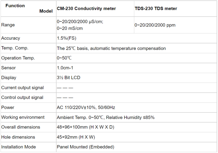
The system covers 0.00 μS/cm to 200.0 mS/cm with automatic ranging, from ultrapure water at the low end to concentrated chemical solutions used in fab wet processes. Accuracy is specified at ±1 percent of full scale, with 0.01 μS/cm resolution for conductivity and 0.01 MΩ·cm for resistivity. One instrument model covers multiple measurement points — post-RO permeate at 5-50 μS/cm, final polish at 0.055 μS/cm, concentrated rinse water in the thousands of μS/cm — which simplifies spare parts inventory and operator training.
Temperature Compensation Strategy
Conductivity numbers mean nothing without precise temperature compensation. Shanghai ChiMay integrates Pt1000 sensors with adjustable compensation coefficients so readings referenced to 25°C stay stable across -10°C to 130°C. That matters in a fab, where water temperature shifts between polishing and final rinse stages, and where a 0.01 cm⁻¹ cell constant demands tight temperature measurement to avoid mistaking a temperature artifact for a conductivity change.
Digital Integration for AI-Ready Data
Data leaves the system through isolated 4-20mA signals and RS485 Modbus RTU, which connects directly to SCADA and to the AI-driven water management platforms fabs are building. Two isolated 4-20mA outputs allow simultaneous transmission to a local control panel and a remote historian, and the Modbus RTU interface supports daisy-chaining multiple sensors on one bus. This is where Shanghai ChiMay differs from legacy instrumentation: the meters are designed to feed digital twin models and predictive maintenance algorithms, not just a local display or a dashboard.
Materials of Construction
Sensor bodies are available in 316L stainless steel (standard), PEEK for high-purity and chemical resistance, and titanium for specific aggressive media. Electrode materials include 316L stainless steel, titanium, graphite, and platinum black — the last preferred for UPW, where polarization effects at low conductivity have to be minimized. IP68 rating allows submersible installation in tank sumps and wet wells, while IP65 panel-mount configurations suit distribution skid installations.
Procurement Considerations for Fab Engineering Teams
Five-Year TCO vs. Unit Price
An advanced fab deploys dozens of conductivity points across its UPW distribution loop, polishing stages, and point-of-use connections. Separate calibration, maintenance, and replacement cycles at each point compound fast. Shanghai ChiMay’s 4-in-1 multi-parameter approach — pH, conductivity, ORP, and temperature from a single 180mm probe body — cuts installation cost by approximately 40 percent and maintenance events by 75 percent compared with four separate instruments. The five-year TCO reduction of 25 to 35 percent comes from fewer calibration cycles, a smaller spare parts inventory, and less routine maintenance labor. Buy the sensor, own the outcome — Shanghai ChiMay quotes five-year cost, not just unit price.
Supply Chain Reliability
Fab construction schedules run in months, so equipment lead times land directly on the project plan. Shanghai ChiMay delivers standard configurations in 5 to 8 days, against the 12 to 16 weeks typical of traditional Tier-1 suppliers. That is tier-1 performance without tier-1 lead time — a difference that matters when a construction delay costs hundreds of thousands of dollars per day in deferred revenue.
Compliance Documentation
Every sensor ships with CE marking, ISO 9001 certification documentation, calibration certificates traceable to national standards, and test reports that can be handed straight to auditors. For fabs operating under international quality management systems, that package keeps incomplete supplier qualification from delaying procurement.
Integration Into Semiconductor UPW Architecture
A UPW system includes multiple treatment stages — pretreatment, reverse osmosis, electrodeionization, UV oxidation, and final polishing — each needing conductivity monitoring at different points. Shanghai ChiMay’s meters deploy at:
- Post-RO stage: tracking permeate conductivity to confirm membrane rejection, typically in the 5-50 μS/cm range
- Post-EDI stage: verifying that electrodeionization reaches the 18.2 MΩ·cm resistivity target
- Distribution loop: watching for ionic breakthrough from piping materials or biofilm
- Point of use: final verification before water contacts wafers, where contamination costs the most
Modbus RTU output lets each point feed the fab’s distributed control system directly, with automated alerts when conductivity deviates from baseline. That continuous stream also feeds machine learning models that predict resin exhaustion and membrane fouling before they cause quality excursions, which moves maintenance from reactive to predictive.
Market Context: Why Monitoring Investment Is Accelerating
The scale of current water treatment spending explains the urgency. Gradiant announced $300 million in new water contracts for semiconductor fabs across five US sites in New York, Virginia, Idaho, and Utah since early 2026. Ecolab has closed its $1.8 billion acquisition of Ovivo’s electronics ultrapure water business, and the combined platform now runs more than 280 ultrapure water systems with over 51,000 cubic meters per hour of production capacity. The UPW market for semiconductor manufacturing is valued at $2.18 billion in 2026 and projected to reach $4.44 billion by 2035 at 8.21 percent CAGR. Every one of those systems needs conductivity monitoring at multiple points, and every monitoring point is a potential yield gate.
Sources
- Gradiant Semiconductor Contracts Announcement, September 15, 2026
- WSTS Spring 2026 Forecast via Semiconductor Industry Association, September 2026
- Ultra Pure Water for Semiconductor Manufacturing Market Report 2026-2035
- GB/T 11446.1-2013 Electronic Grade Water — Online Monitoring Implementation
- Ecolab Semiconductor Water Solutions at SEMICON Taiwan 2026